










 EN
EN ZH
ZHWhat is an Epitaxial Wafer?
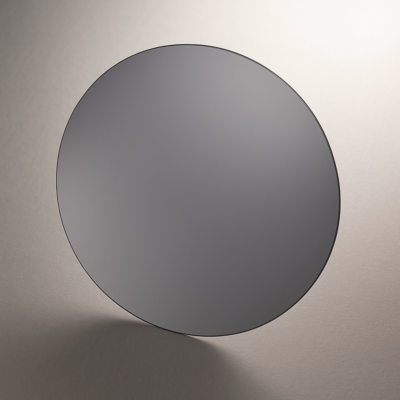
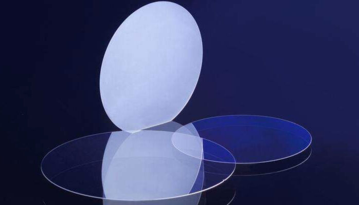
An epitaxial wafer, commonly referred to as an EPI wafer, is a semiconductor substrate on which a thin crystalline layer of silicon is grown through a controlled epitaxial deposition process. The grown layer maintains the same crystal orientation as the underlying substrate, forming a continuous and defect-controlled crystal structure.
In semiconductor manufacturing, the epitaxial layer is typically deposited on a highly polished silicon wafer. This process allows engineers to precisely control important electrical parameters such as dopant concentration, resistivity, and layer thickness, enabling the fabrication of advanced semiconductor devices.
Depending on the application, the epitaxial layer thickness can range from sub-micron levels to several tens of micrometers, allowing device designers to tailor electrical characteristics for specific applications.
Epitaxial Growth Process
The epitaxy process involves the deposition of semiconductor material onto a single-crystal substrate while preserving its crystallographic orientation. This technique enables the growth of extremely uniform semiconductor layers with tightly controlled electrical and structural properties.
Several epitaxial growth technologies are widely used in the semiconductor industry, including:
• Chemical Vapor Deposition (CVD)
• Metal-Organic Chemical Vapor Deposition (MOCVD)
• Molecular Beam Epitaxy (MBE)
Among these methods, CVD-based epitaxy is commonly used for silicon epitaxial wafers due to its ability to produce high-quality layers with excellent thickness and doping uniformity.
Key Benefits of Epitaxial Silicon Wafers
Epitaxial wafers offer several technical advantages compared to conventional silicon wafers.
Superior Crystal Quality
The epitaxial layer grows directly from the substrate lattice, resulting in excellent crystal continuity and significantly reduced defect density. This high crystal quality is essential for reliable semiconductor device operation.
Accurate Doping Control
During epitaxial growth, dopants can be introduced with precise concentration levels. This allows manufacturers to design semiconductor structures with carefully engineered electrical characteristics.
Enhanced Electrical Performance
Devices fabricated on epitaxial wafers often demonstrate improved electrical performance, including lower leakage current, better breakdown voltage control, and enhanced switching efficiency.
Flexible Device Design
By combining different substrate properties with tailored epitaxial layers, semiconductor engineers can design complex device structures that cannot be achieved using bulk wafers alone.
Applications of Epitaxial Wafers
Epitaxial silicon wafers are widely used across multiple sectors of the semiconductor industry.
Power Semiconductor Devices
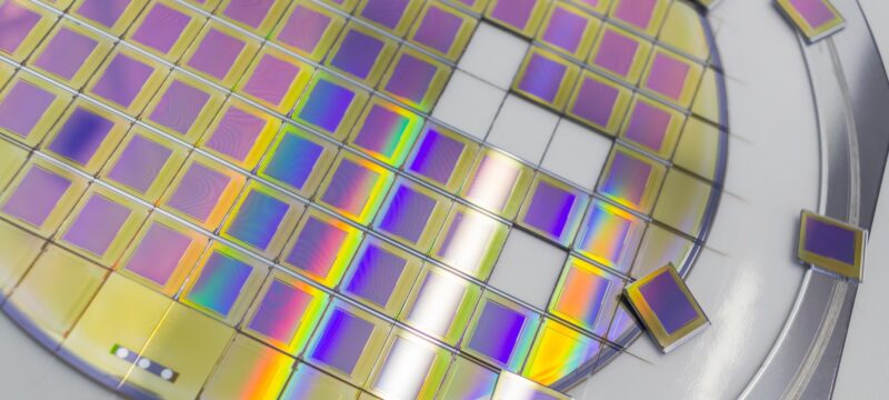
Epitaxial wafers play an essential role in power electronics. They are commonly used in the fabrication of MOSFETs, IGBTs, power rectifiers, and high-voltage diodes.
Integrated Circuits (IC)
In advanced integrated circuit manufacturing, epitaxial wafers are used to optimize transistor structures, reduce parasitic effects, and improve overall device performance.
RF and Communication Devices
Many radio-frequency components and communication chips rely on epitaxial structures to achieve the high frequency response and low noise characteristics required in modern wireless technologies.
Optoelectronic Devices
Epitaxial growth techniques are also fundamental in optoelectronics, including the production of LEDs, laser diodes, optical sensors, and photonic devices.
Photovoltaic Technologies
Certain high-efficiency solar cell designs utilize epitaxial silicon layers to enhance light absorption and carrier transport efficiency.
Typical Structure of an Epitaxial Wafer
An epitaxial wafer generally consists of two primary components:
- Substrate wafer – Provides mechanical support and base crystal orientation
• Epitaxial layer – Active semiconductor layer with controlled electrical properties
The substrate ensures structural stability, while the epitaxial layer determines the electrical behavior required for device fabrication.
Future Outlook
As semiconductor technologies continue to evolve toward higher power density, improved energy efficiency, and increased integration, the importance of epitaxial wafer technology continues to grow.
Epitaxial silicon wafers are now widely used in applications ranging from automotive electronics and power modules to communication systems and consumer electronics. The ongoing development of advanced semiconductor devices will further increase the demand for high-quality epitaxial wafer materials.
Epitaxial Wafer Supply
With extensive experience in semiconductor material supply, we provide high-quality epitaxial silicon wafers tailored to a wide range of device applications. Custom specifications including wafer diameter, doping type, resistivity range, and epitaxial layer thickness can be supported according to customer requirements.
If you are looking for a reliable epi wafer supplier for semiconductor applications, please feel free to contact our team for further discussion. We maintain stock of 4″, 6″, 8″, and 12″ epitaxial wafers for small-quantity supply, and we can also support custom specifications for mass production.


