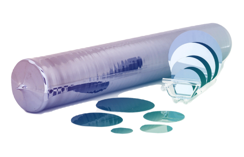
Silicon wafers are integral to technological advancement, and our company excels in delivering a wide array tailored to diverse specifications.
Our offerings encompass dummy to prime grades with particle control up to 15nm, available in various types and specifications for customized needs.
Standard bare silicon wafers are ready for immediate shipping, while most of custom specifications orders are processed and shipped within four weeks.
Partner with us for reliable access to silicon wafers that meet the highest standards of quality and customization.

Bare Silicon Wafers

Swift Delivery

Small Quantities Welcome

High Quality
01. DUMMY WAFER (COINROLL WAFER)
Dummy wafers are crucial for safety at the production outset, employed in delivery checks and process evaluations. Our strength lies in 2 to 12-inch dummy wafers with diverse thicknesses and surface finishes. Specifically, for standard specifications, we guarantee an always-in-stock status with competitive prices, ensuring swift order fulfillment.

Standard specifications
| Specifications | 2” | 3” | 4” | 5” | 6” | 8” | 12” |
| Diameter (mm) | 50.8±0.5 | 76.0±0.5 | 100±0.5 | 125±0.5 | 150±0.5 | 200±0.5 | 300±0.5 |
| Type/Dopant: | P/Boron or N/Ph | P/Boron or N/Ph | P/Boron or N/Ph | P/Boron or N/Ph | P/Boron or N/Ph | P/Boron or N/Ph | P/Boron or N/Ph |
| Thickness (μm) | 280±25 | 380±25 | 525±25 | 625±25 | 625±25/675±25 | 725±25 | 775±25 |
| Flat/Notch | Flats | Flats | Flats | Flats | Flats/Notch | Flats/Notch | Notch |
| Surface Finish | As-Cut/Lapped/Etched/SSP/DSP | As-Cut/Lapped/Etched/SSP/DSP | As-Cut/Lapped/Etched/SSP/DSP | As-Cut/Lapped/Etched/SSP/DSP | As-Cut/Lapped/Etched/SSP/DSP | As-Cut/Lapped/Etched/SSP/DSP | As-Cut/Lapped/Etched/SSP/DSP |
SPECIAL SPECIFICATIONS
| Specifications | 8” | 12” |
| Diameter (mm) | 200±0.5 | 300±0.5 |
| Thickness (μm) | >680/>700/>1000 | >800/>1000/>1300 |
| Flat/Notch | Flats/Notch | Notch |
| Surface Finish | As-Cut/Lapped/Etched/SSP/DSP | As-Cut/Lapped/Etched/SSP/DSP |
02. PARTICLE CONTROL WAFER
Particle Control Wafers, commonly known as dust-free wafers. A standard box contains 25 wafers, vacuumed and sealed for protection. These wafers fall into three categories: Test, Monitor, and Prime Grades.
Test and Monitor wafers are designed for research and early production, while Prime Wafers offer exceptional quality with advanced particle control and flatness. They are particularly well-suited for intricate projects such as photolithography or direct IC chip production, playing a crucial role in forming circuit patterns on substrates and manufacturing devices.
Test and Monitor wafers are designed for research and early production, while Prime Wafers offer exceptional quality with advanced particle control and flatness. They are particularly well-suited for intricate projects such as photolithography or direct IC chip production, playing a crucial role in forming circuit patterns on substrates and manufacturing devices.
Test Grade Specifications
| Specifications | 2inch Test Grade | 3inch Test Grade | 4inch Test Grade | 6inch Test Grade | 8inch Test Grade | 12inch Test Grade |
| Diameter | 50.8±0.38mm | 76.2±0.63mm | 100±0.2mm | 150±0.2mm | 200±0.2mm | 300±0.2mm |
| Growth Method | CZ | CZ | CZ | CZ | CZ | CZ |
| Orientation | <100> | <100> | <100> | <100> | <100> | <100> |
| Type/Dopant | P/Boron | P/Boron | P/Boron | P/Boron | P/Boron | P/Boron |
| Resistivity | 1-100 ohm.cm | 1-100 ohm.cm | 1-100 ohm.cm | 1-100 ohm.cm | 1-100 Ω/cm | 1-100 Ω/cm |
| Surface Finish | Polished/Etched | Polished/Etched | Polished/Etched | Polished/Etched | Polished/Etched | Polished/Polished |
| Thickness | 279±25μm | 381±25μm | 525±25μm | 625/675±25μm | 725±25μm | 775±25μm |
| TTV | ≤10um | ≤10um | ≤10um | ≤10μm | ≤10μm | ≤10μm |
| BOW/WARP | <40μm | <40μm | <40μm | <40μm | <40μm | <40μm |
| Particle | 0.3μm≤10ea | 0.3μm≤10ea | 0.3μm≤10ea | 0.3μm≤10ea | 0.3μm≤10ea | 0.3μm≤10ea |
| Time of Shipment | Immediate Shipment | Immediate Shipment | Immediate Shipment | Immediate Shipment | Immediate Shipment | Immediate Shipment |
For 8-inch and 12-inch sizes, we are also able to provide
different particle control depending on your applications.
| Specifications | 300mm@15nm | 300mm@26nm | 300mm@37nm | 300mm@45nm | 300mm@65nm | 300mm@90nm | 300mm@200nm | 200mm@200nm | 200mm@160nm | 200mm@200nm |
| Diameter | 300±0.2mm | 300±0.2mm | 300±0.2mm | 300±0.2mm | 300±0.2mm | 300±0.2mm | 300±0.2mm | 200±0.2mm | 200±0.2mm | 200±0.2mm |
| Growth Method | CZ | CZ | CZ | CZ | CZ | CZ | CZ | CZ | CZ | CZ |
| Orientation | <100> | <100> | <100> | <100> | <100> | <100> | <100> | <100> | <100> | <100> |
| Type/Dopant | P/Boron | P/Boron | P/Boron | P/Boron | P/Boron | P/Boron | P/Boron | P/Boron | P/Boron | P/Boron |
| Resistivity | 1-100 Ω/cm | 1-100 Ω/cm | 1-100 Ω/cm | 1-100 Ω/cm | 1-100 Ω/cm | 1-100 Ω/cm | 1-100 Ω/cm | 1-100 Ω/cm | 1-100 Ω/cm | 1-100 Ω/cm |
| Surface Finish | Polished/Polished | Polished/Polished | Polished/Polished | Polished/Polished | Polished/Polished | Polished/Polished | Polished/Polished | Polished/Etched | Polished/Etched | Polished/Etched |
| Thickness | 775±5μm | 775±5μm | 775±5μm | 775±5μm | 775±5μm | 775±5μm | 775±5μm | 725±5μm | 725±5μm | 725±5μm |
| TTV | ≤1μm | ≤1μm | ≤1μm | ≤1μm | ≤3μm | ≤5μm | ≤10μm | ≤2μm | ≤10μm | ≤10μm |
| BOW/WARP | <30μm | <30μm | <30μm | <30μm | <30μm | <40μm | <40μm | <30μm | <40μm | <40μm |
| Particle | 0.015μm≤50ea | 0.026μm≤100ea | 0.037μm≤70ea | 0.045μm≤50ea | 0.065μm≤50ea | 0.09μm≤50ea | 0.2μm≤50ea | 0.2μm≤30ea | 0.16μm≤50ea | 0.2μm≤50ea |
| Lasermark | T7/M12 | T7/M12 | T7/M12 | T7/M12 | T7/M12 | T7/M12 | T7/M12 | None Laser Scribe | None Laser Scribe | None Laser Scribe |
| Others | Notch | Notch | Notch | Notch | Notch | Notch | Notch | Notch | Notch | Notch |
| Time of Shipment | Immediate Shipment | Immediate Shipment | Immediate Shipment | Immediate Shipment | Immediate Shipment | Immediate Shipment | Immediate Shipment | Immediate Shipment | Immediate Shipment | Immediate Shipment |