








 EN
EN JA
JAIn semiconductor manufacturing, adhesive tapes play a crucial role in processes such as wafer
dicing, back grinding, and chip handling. These tapes temporarily secure the wafer during
processing, helping to protect delicate structures and maintain precise positioning. Among the
most commonly used options are UV tapes and non-UV tapes. While both are designed to hold
wafers firmly in place, their behavior during removal differs. Choosing the right type of tape can
greatly influence production efficiency, yield, and product reliability.
The Role of Tape in Wafer Processing
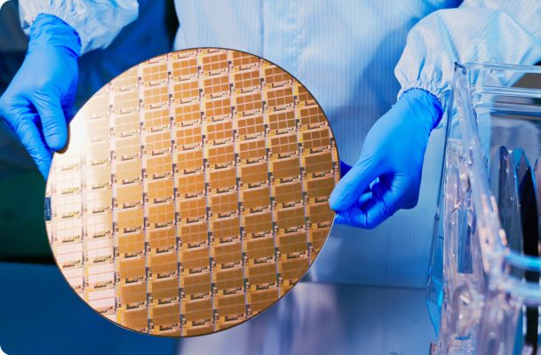
After front-end fabrication steps such as etching and metallization, wafers must undergo
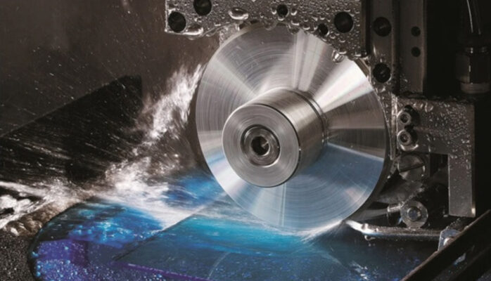
mechanical processes like back grinding and dicing. During these steps, the wafer is mounted
onto an adhesive tape stretched over a frame. This tape supports the wafer, prevents
movement, and keeps individual dies aligned after cutting. Without proper tape performance,
wafers may crack, chips can shift, and valuable devices may be damaged.
Non-UV tape is a standard adhesive tape that maintains strong bonding throughout the entire
process. It provides stable holding force during grinding and dicing, making it suitable for thicker
or more robust wafers. However, because its adhesive strength does not change, removing the
tape requires mechanical peeling. This can induce stress to the wafer or dies and may leave
adhesive residue on the surface. For applications involving fragile or ultra-thin wafers, this
increased stress can result in chipping, cracking, or contamination.
UV tape, on the other hand, is engineered with a special adhesive that responds to UV light.
Before UV exposure, it behaves similarly to non-UV tape, providing strong adhesion to secure
the wafer during processing. After UV irradiation, the adhesive strength drops dramatically,
allowing the tape to be removed easily and cleanly. This low-stress release helps protect
delicate chips and minimizes the risk of damage or residue. For modern semiconductor
manufacturing, where wafers are becoming thinner and die sizes smaller, UV tape has become
an essential material.
Choosing the Right Tape for Your Process
The decision between UV and non-UV tape depends on the specific requirements of the
manufacturing process. For thick wafers or less sensitive applications, non-UV tape may offer a
cost-effective and simple solution. For advanced processes involving thin wafers, fine-pitch
dicing, or high-value devices, UV tape provides superior protection and cleaner debonding. In
high-yield environments, the reduced risk of damage offered by UV tape can lead to significant
improvements in overall production quality.
The Importance of High-Quality TapeJust as wafer quality affects chip performance, tape quality directly influences processing
stability and product yield. Poor adhesion uniformity, inconsistent thickness, or weak mechanical
properties can lead to wafer movement, die misalignment, and surface contamination.
High-quality semiconductor tapes are designed with controlled adhesive strength, excellent
tensile properties, and consistent thickness to ensure reliable performance throughout the
manufacturing process.
At D&X, we understand the critical role that tape plays in protecting wafers and maintaining chip
integrity. The UV and non-UV tapes we supply provide stable adhesion during processing and
clean, low-residue release after use, helping to reduce wafer damage during back grinding and
dicing. With customizable solutions tailored to each customer’s requirements, we ensure optimal
performance for a wide range of semiconductor applications.


