






 EN
EN JA
JA
From Wafer to Chip: The Importance of Dicing
The production of integrated circuit (IC) chips involves several complex steps, starting from the fabrication of silicon wafers to the creation of individual semiconductor devices. One of the most vital processes in this process is dicing, where a completed wafer is carefully sliced into thousands of separate chips. This step requires exceptional accuracy and care to prevent damage and ensure the highest yield. Suppliers and manufacturers such as D&X provide high-quality silicon wafers designed to endure the demands of dicing and subsequent processing, enabling semiconductor manufacturers to produce reliable, high-performance chips for modern electronics.
The Dicing Process
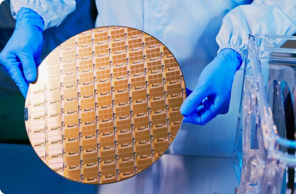
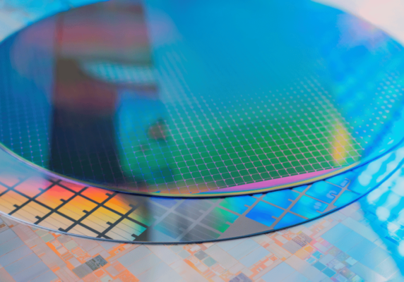
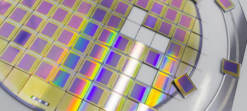
After the intricate fabrication steps have been completed on a silicon wafer (photolithography, etching, and metallization), the wafer is still a single large disc containing many identical circuit patterns. To create individual IC chips, the wafer must be divided into separate dies by a process known as dicing. Dicing involves cutting the wafer along pre-defined scribe lines with high precision to avoid damaging the fragile circuitry.
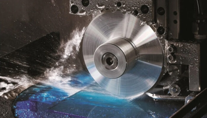
There are two primary dicing methods: mechanical sawing and laser dicing. Mechanical sawing utilizes a diamond-tipped blade to carefully slice through the wafer. This traditional method is highly reliable and widely used, but it can introduce mechanical stress and generate particles requiring thorough cleaning afterward. Laser dicing, on the other hand, employs focused laser beams to ablate or cut the silicon without physical contact. This reduces mechanical stress and is particularly advantageous for very thin or delicate wafers, as well as for advanced packaging techniques that require narrower cut widths.
During the dicing operation, the wafer is mounted on a sticky film or adhesive tape (dicing tape), which holds the individual dies in place once the cuts are made. This ensures that chips remain secure and organized, facilitating downstream handling and packaging processes.
Transformation into IC Chips
Once separated, each individual die undergoes a series of backend processing steps to transform it into a finished integrated circuit chip. These steps include die inspection, testing, packaging, and final qualification.
Die inspection screens for any damage or defects resulting from fabrication or dicing. Only dies that meet rigorous standards proceed to packaging, where the tiny silicon chip is mounted onto a substrate or lead frame. Connections between the die’s bonding pads and external circuitry are made using wire bonding or flip-chip techniques. This packaging step protects the die from physical and environmental damage while enabling electrical integration into larger electronic systems.
Subsequent testing ensures that the chips operate correctly under expected conditions and meet performance specifications. The finished IC chips are then ready for shipment to electronics manufacturers worldwide, where they become essential components in devices ranging from smartphones to automotive systems.
The Importance of Quality Wafers
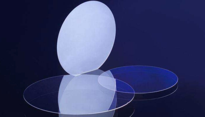
The success of dicing and subsequent chip fabrication depends greatly on the quality of the starting silicon wafers. Wafers supplied by D&X are manufactured with strict quality controls to ensure excellent surface smoothness, uniform thickness, and minimal defects. Such precision helps prevent wafer cracking, die chipping, and other issues that can arise during dicing and handling.
By sourcing wafers optimized for downstream processing, manufacturers can improve outcomes and produce more reliable integrated circuits. This collaboration between wafer suppliers and chip manufacturers drives ongoing innovation in the semiconductor industry.


