









 ZH
ZH JA
JA
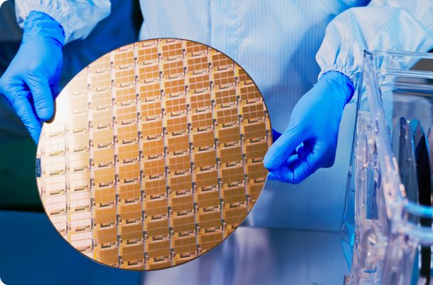
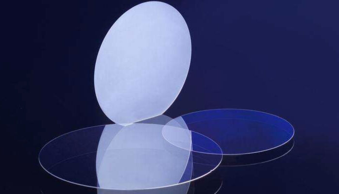
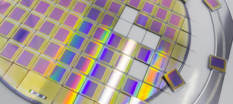
At D&X, with a focus on Silicon Carbide wafers, goes beyond supplying compound materials. We boast several production lines dedicated to Silicon Carbide wafers, leveraging our established expertise to meet your specific requirements.
Our confidence in satisfying your needs stems from our long-standing commitment to excellence. With a proven track record and in-depth knowledge of these advanced materials' applications, D&X stands as a reliable partner in the semiconductor industry. The combination of our established production lines and specialized expertise positions us at the forefront of delivering cutting-edge semiconductor solutions.
Refer to our Stock List for currently available specifications.

Compound Semiconductor

Swift Delivery

Small Quantities Welcome

High Quality
01. COMPOUND SEMICONDUCTOR
Our confidence in satisfying your needs stems from our long-standing commitment to excellence. With a proven track record and in-depth knowledge of these advanced materials' applications, D&X stands as a reliable partner in the semiconductor industry. The combination of our established production lines and specialized expertise positions us at the forefront of delivering cutting-edge semiconductor solutions.

Silicon Carbide (SiC) Wafer Specifications
| Grade | Zero MPD | Production | Research Grade | Dummy Grade | |
| Diameter | 50.8 ±0.38 mm // 76.2 ±0.38 mm // 100+0.5 mm // 150±0.25mm | ||||
|
Thickness
|
4H-N | 350μm ± 25μm | |||
|
Thickness
|
4H-SI | 500μm ± 25μm | |||
| Wafer Crystal Orientation | Off axis:4.0° toward 1120! ± 0.5° for 4H-N On axis: <0001> ± 0. 5° for 4H-SI | ||||
| Micropipe Density | <1cm-2 | <5cm-2 | <15cm-2 | <50cm-2 | |
|
Resistivity
|
4H-N | 0.015 ~ 0.028ohm-cm | |||
|
Resistivity
|
6H-N | 0.02 ~ 0.1ohm-cm | |||
|
Resistivity
|
4/6H-SI | >1E5Q-cm (90%) | >1E5Q-cm | ||
| Primary Flat | {10-10} ± 5.0° | ||||
| Primary Flat Length | 15.9 mm ± 1.7 mm // 22.2 mm ± 3.2 mm // 32.5 mm ± 2.0 mm // 47.5 mm ± 2.5mm | ||||
| Secondary Flat Length | 8.0 mm ± 1.7 mm // 11.2 mm ± 1.5 mm, 18.0mm ± 2.0 mm // —– | ||||
| Secondary Flat Orientation | Silicon face up: 90° CW from Prime flat ± 5.0° | ||||
Indium Phosphide (InP) Specifications
| Growth Method | VGF | ||
| Type/Dopant | Undoped // N/S/Sn // P/Zn | ||
| Size | 2inch | 3inch | 4inch |
| Diameter (mm) | 50.8±0.3 | 76.2±0.3 | 100±0.3 |
| Thickness (um) | 350±25 | 625±25 | 625±25 |
| OF(mm) | 16±2 | 22±2 | 32.5±2 |
| IF(mm) | 8±2 | 12±2 | 18±2 |
| Orientation | (100)±0.5 | ||
| TTV(um) | ≦10 | ≦15 | ≦15 |
| Bow(um) | ≦15 | ≦15 | ≦15 |
| Wrap(um) | ≦15 | ≦15 | ≦15 |
| Surface | Polished/Etched | ||
| Epi-ready | Yes | ||
Gallium Arsenide (GaAs) Wafer Specification
| Diamter | 50 ~ 150mm ± 0.25mm(2″ // 3″ // 4″ // 6″) |
| Material | Single Crystal Gallium Arsenide |
| Growth Method | VGF // LEC Grown |
| Crystal Orientation | <100> // <111> |
| Crystal Orientation | α 0 ± β 0, off angle α and accuracy β upon request |
| Dopant | Undoped // Zn // Si // Te |
| Thickness | 350 ± 25um // 550 ± 25um // 625 ± 25um |
| Mobility | 1500 ~ 3000 // 3000 ~ 5000 cm2 / V·sec |
| Primary Flat | <0-1-1> ± 0.5deg, 16 ±1.0mm // 22±1.0mm // 32.5±1.0mm |
| Secondary Flat | <0-1-1> ± 5.0 deg, 8 ±1.0mm // 11±1.0mm // 18±1.0mm |
| Front-side | Polished in Epi-ready Prime grade |
| Back-side | Polished / Lapping or Etched |
| Epi-ready | Yes |
Germanium (Ge) Wafer Specifications
| Diameter | 2 inch ~ 6 inch | ||
| Thickness | 175um // 200um / 400um // 500um // 625um | ||
| Type/Dopant | Undoped | N/Sb | P/Ga |
| Resistivity (Ω・cm) | >30 | >0.005 | >0.005-0.04 |
| EP(/cm2) | <3000 | <3000 | 0 |
| Orientation | <100> // <111> | ||
| TTV | ≤25μm | ||
| Bow | ≤25μm | ||
| Wrap | ≤25μm | ||
| Surface | E/E // P/E // P/D | ||
| Epi-ready | Yes | ||
Indium Antimonide (InSb) Wafer Specifications
| Growth Method | VGF | |
| Type/Dopant | Undoped // N/S/Sn // P/Zn | |
| Diameter(mm) | 50.8 ± 0.3 | 76.2 ± 0.3 |
| Thickness(um) | 500 ± 25 | 650 ± 25 |
| OF(mm) | 16 ± 2 | 22 ± 2 |
| IF(mm) | 8 ± 2 | 12 ± 2 |
| Orientation | <100> | |
| TTV(um) | ≤10 | ≤15 |
| Bow(um) | ≤15 | ≤15 |
| Wrap(um) | ≤15 | ≤15 |
| Surface | Polished/Etched | |
| Epi-ready | Yes | |
Indium Arsenide (InAs) Wafer Specifications
| Growth Method | VGF | ||
| Type/Dopant | Undoped // N/S/Sn // P/Zn | ||
| Diameter(mm) | 50.8 ± 0.3 | 76.2 ± 0.3 | 100 ± 0.3 |
| Thickness(um) | 500 ± 25 | 600 ± 25 | 800 ± 25 |
| OF(mm) | 16 ± 2 | 22 ± 2 | 32.5 ± 2 |
| IF(mm) | 8 ± 2 | 12 ± 2 | 18 ± 2 |
| Orientation | <100> // <111> | ||
| TTV(um) | ≤10 | ≤10 | ≤15 |
| Bow(um) | ≤10 | ≤10 | ≤15 |
| Wrap(um) | ≤15 | ≤15 | ≤15 |
| Surface | Polished/Etched | ||
| Epi-ready | Yes | ||
Gallium Nitride (GaN) Wafer Specifications
| Growth Method | HVPE | ||
| Conduct Type | Semi-Insulating | N | N |
| Type/Dopant | Fe | Ge | Undoped |
| Size | 10×10.5mm // 100.5 ± mm | ||
| OF location/length | <1-100> ± 0.5° // 32.0 ± 1.0mm | ||
| IF location/length | <11-20> ± 3° // 18.0 ± 1.0mm | ||
| Orientation | C-plane<0001> off angle toward M-Axis 0.35° ± 0.15mm | ||
| Resistivity(300k) | ≧1E6 ohm-cm <0.05ohm.cm <0.5ohm.cm | ||
| EPD | (1 ~ 9)E5/cm2 5E5 ~ 3E6/cm2 (1 ~ 3)E6/cm2 | ||
| Ra(nm) | Frount surface Ra ≤0.2nm | ||
| TTV(um) | ≤ 15 | ||
| Bow(um) | ≤ 20 | ||
| Wrap(um) | ≤ 20 | ||
| Epi-ready | Yes | ||