





 ZH
ZH JA
JAThin film deposition is a way to coat a surface with an extremely thin layer of material. These films can change a surface’s electrical, optical, mechanical, and chemical behavior, which is why they are essential in semiconductor manufacturing. This guide first explains what thin films are and why we use them. It then introduces the three common deposition categories—PVD, CVD, and ALD—and focuses on PVD (Physical Vapor Deposition).
- Thin Film Deposition
1.1 What is Thin Film Deposition?
Thin film deposition is a way to coat a surface with a very thin layer of material (a “thin film”).
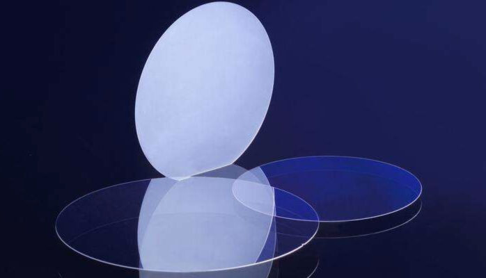
The surface being coated is called the substrate (for example: a silicon wafer, glass, or plastic).
1.2 What can thin films be made of?
Thin films can be made from many materials, such as:
- Metals (aluminum, copper, titanium)
- Oxides (silicon dioxide)
- Other compounds (nitrides)
1.3 Why add a thin film?
A thin film can improve a surface by changing its:
- Optical properties (transmit, block, or reflect light)
- Electrical properties (conduct, insulate, or control electrical signals / electric current)
- Mechanical durability (harder, more wear- and scratch-resistant)
- Chemical resistance (better resistance to corrosion and chemicals)
1.4 Where is thin film deposition used?
Thin film deposition is used in many products and industries, including (but not limited to):
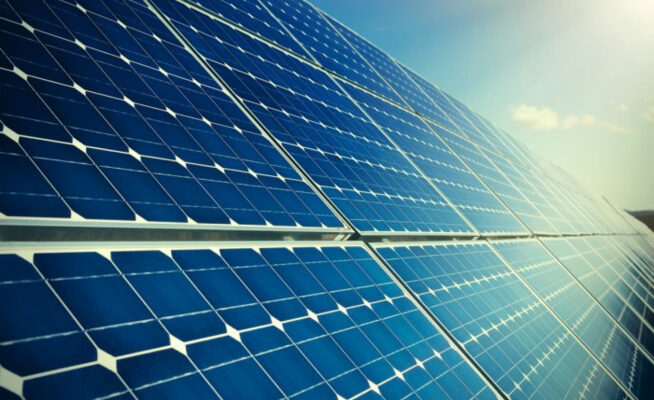
- Semiconductors and electronics
- LEDs and displays
- Lasers and optical parts (filters, lenses, precision optics)
- Medical devices (implants and protective coatings)
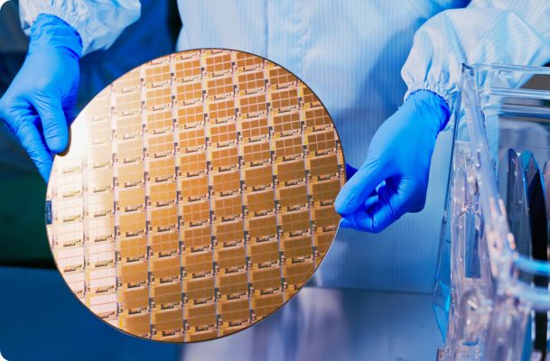
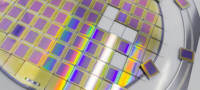
This guide focus on semiconductor processing, where thin films are deposited on wafer substrates—most commonly silicon wafers—to build device layers.
- Three Types of Thin Film Deposition
For a beginner-friendly overview, deposition methods are often grouped into two main types: PVD (Physical Vapor Deposition) and CVD (Chemical Vapor Deposition). In semiconductor manufacturing, a third category is often added: ALD (Atomic Layer Deposition).
With that context, this guide will focus on Physical Vapor Deposition.
- What is Physical Vapor Deposition (PVD)?
PVD is a family of thin-film deposition methods usually performed in a vacuum chamber.
Most PVD processes follow the same basic steps:
- Release atoms from a source material
- Transport them through vacuum (or low pressure gas)
- Deposit and grow a thin film on the substrate
On silicon wafers, PVD is most commonly used to deposit metal films (e.g., for interconnects, contacts, barrier/adhesion layers, and seed layers).
3.1 Main Types of Physical Vapor Deposition (PVD)
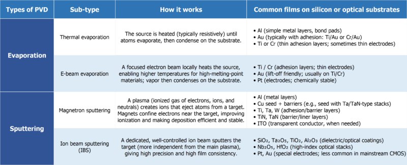
PVD methods are often grouped by how atoms are released:
3.1.1 Evaporation
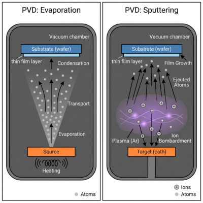
Evaporation methods heat a material until atoms (or molecules) escape from its surface as vapor, then that vapor travels to the substrate and condenses to form a thin film. There are two types:
- Thermal evaporation
- E-beam evaporation
3.1.2 Sputtering
Sputtering uses ion bombardment: ions hit a target and knock atoms off. Those atoms then deposit on the substrate.
- Magnetron sputtering
- Ion beam sputtering (IBS)