









 ZH
ZH JA
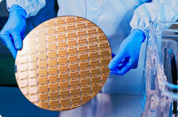
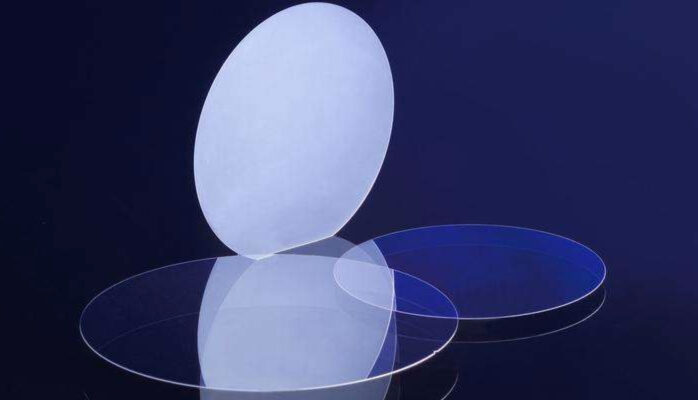
JAHigh-resistivity (HR) substrate wafers play an important role in modern semiconductor manufacturing, especially in applications that demand excellent electrical isolation, low signal loss, and strong high-frequency performance.
Compared with conventional low- or medium-resistivity silicon substrates, HR wafers exhibit unique electrical properties that make them essential for RF, power, MEMS, and advanced integration technologies.
The most notable characteristic of high-resistivity substrates is their extremely high bulk resistivity, typically ranging from 1 kΩ·cm to over 10 kΩ·cm. This high resistivity, achieved through ultra-low doping or intrinsic silicon, effectively suppresses parasitic conduction paths, reducing leakage current and substrate coupling effects.
At high frequencies, high-resistivity wafers demonstrate significantly lower substrate loss. Reduced dielectric loss and minimized eddy current generation help limit signal attenuation, making these substrates well suited for GHz and millimeter-wave applications where signal integrity is critical.
High-resistivity substrates also provide excellent electrical isolation between devices on the same wafer. This reduces cross-talk, improves signal integrity, and enhances overall circuit performance, which is particularly important in highly integrated RF front-end and mixed-signal circuits.
When properly processed, HR wafers offer stable electrical performance across a wide temperature range. Although surface states and interface charges can influence effective resistivity, appropriate surface treatment and passivation techniques can maintain reliable and consistent electrical behavior.
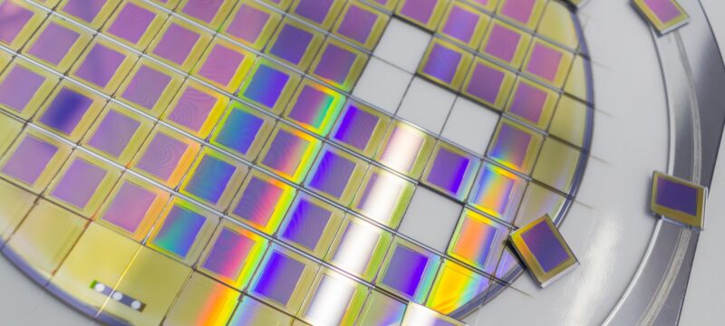
Due to these advantages, high-resistivity substrates are widely used in RF and microwave devices such as RF switches, LNAs, PAs, and RF front-end modules. They are also key components of RF-SOI structures, where high-resistivity handle wafers work with buried oxide layers to further improve isolation and suppress substrate leakage.
In power semiconductor applications, high-resistivity substrates help manage electric field distribution and reduce leakage currents, supporting power management ICs and certain high-voltage device structures. Additionally, MEMS and sensor devices—including microphones, pressure sensors, inertial sensors, and optical detectors—benefit from the low noise and high isolation provided by HR wafers.
With the rise of advanced packaging and heterogeneous integration, high-resistivity substrates are increasingly used as interposers or carrier wafers to reduce signal interference in high-speed and high-frequency systems.
Overall, high-resistivity substrate wafers combine high bulk resistivity, low RF loss, strong isolation, and stable electrical performance. As semiconductor technologies continue to move toward higher frequencies and greater integration, the importance of high-resistivity substrates will continue to grow.


