






 ZH
ZH JA
JA
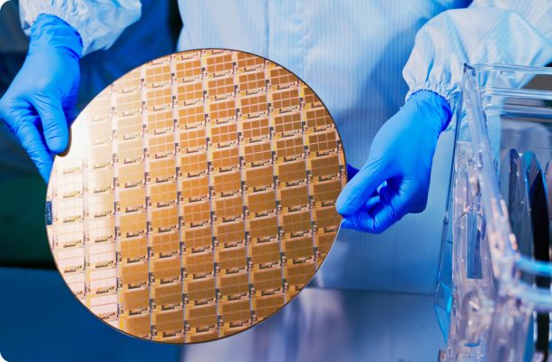
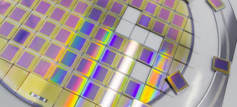
Silicon wafers are the starting point for virtually every semiconductor device, from memory chips to sensors and processors. The process of making these wafers involves multiple precise steps to ensure the surface is flat, pure, and ready for high-end device fabrication. At D&X, we produce wafers with accurate standards, designed to meet the strict cleanliness and quality expectations of today’s semiconductor industry.
From Ingot to As-Cut Wafers
The process begins with the creation of a silicon ingot, which is a large, solid cylinder made of ultra-pure single-crystal silicon. This is typically grown using the Czochralski method, where a seed crystal is dipped into molten silicon and slowly pulled upwards while rotating. The result is a monocrystalline ingot with a specific crystal orientation and very low impurity levels.
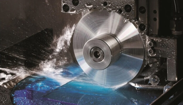
Once the ingot is ready, it is ground to the desired diameter and orientation marks are added. It is then sliced into thin circular wafers using a high-precision wire saw. These slices, called as-cut wafers, have uneven surfaces and saw marks from the slicing process. At this point, the wafers are still too rough for any semiconductor process.
Lapping, Etching, and Polishing
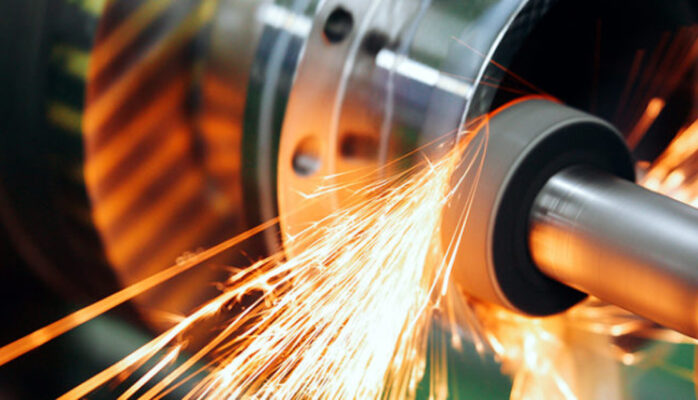
To remove surface damage and improve flatness, the as-cut wafers go through lapping procedure, a grinding process that uses abrasive slurry to smooth out thickness variations. Lapped wafers are flatter but still contain microscopic scratches and residual stress.
Next, wafers are chemically etched to remove the top damaged layer left by lapping. This step also helps relieve surface stress and prepares the wafer for polishing. The etching solution is carefully chosen based on wafer type and desired removal rate.
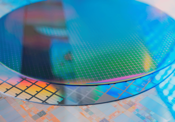
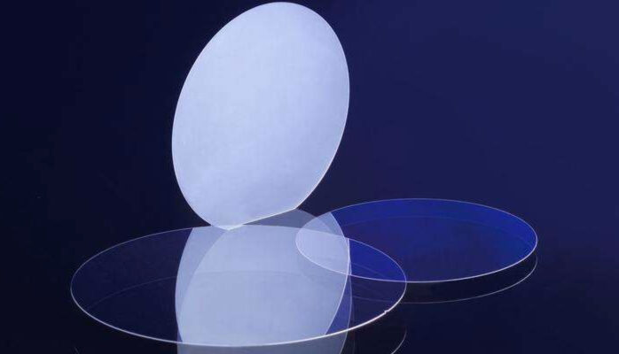
After etching, wafers are ready for chemical-mechanical polishing (CMP). This is a critical step where a combination of soft pads and chemical slurry is used to produce a super-flat, mirror-like surface. CMP removes the final few microns of material, ensuring atomic-level flatness and minimal surface defects. A well-polished wafer is essential for modern semiconductor processes that rely on extreme precision.
Cleaning, Dust-Free Packing, and Final Delivery
After polishing, wafers are cleaned using ultra-pure water and filtered chemicals to remove any trace contaminants or particles. They are then dried and inspected for physical and electrical properties, including thickness, bow, warp, resistivity, and crystal orientation. Wafers that meet customer specifications are sorted and packed.
Before shipping, wafers undergo final cleaning and are labeled as DF (Dust Free). This indicates the wafers have been packed in a cleanroom environment, free from airborne particles that could compromise performance in later processes.
More than just shaping silicon, the wafer manufacturing process is about creating a stable, clean, and precise platform for the entire electronics ecosystem. Whether the end application is logic, power, or memory, the reliability of every device starts with a quality wafer. D&X is committed to supporting that foundation with wafers that meet the industry’s highest expectations.


