
- About us
- Products & Services
- Silicon wafer
-
 Bare Silicon Wafers
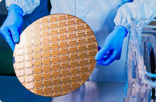
Silicon wafers are integral to technological advancement, and our company excels in delivering a wide array tailored to diverse specifications.
Bare Silicon Wafers
Silicon wafers are integral to technological advancement, and our company excels in delivering a wide array tailored to diverse specifications.
-
 SOI wafer
Silicon on Insulator (SOI) represents a breakthrough in semiconductor wafer technology, outperforming traditional bulk silicon methods.
SOI wafer
Silicon on Insulator (SOI) represents a breakthrough in semiconductor wafer technology, outperforming traditional bulk silicon methods.
-
Compound Semiconductor
At D&X, with a focus on Silicon Carbide wafers, goes beyond supplying compound materials.
-
- Tape
-
Back-Grinding Tape
Strong adhesion to prevent water damage, no adhesive residue keeps adherends clean, especially flat to help with grinding, can be used with uneven surfaces (bump wafers).
-
 Dicing Tape
Strong adhesion to prevent water damage, no adhesive residue keeps adherends clean, especially flat to help with grinding, can be used with uneven surfaces (bump wafers).
Dicing Tape
Strong adhesion to prevent water damage, no adhesive residue keeps adherends clean, especially flat to help with grinding, can be used with uneven surfaces (bump wafers).
-
Bumped Tape
Reduced warping for ultra-thin grinding, heat resistance during grinding/polishing, can protect films for long periods and from heat, antistatic properties when peeling, chemical, acid and base resistance, protective function for high bumps.
-
- Other materials and products
-
Quartz Wafer
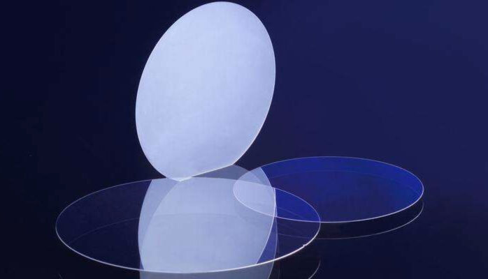
Quartz wafers are made from a type of crystalline silicon dioxide (SiO2). These wafers serve as a crucial material in various high-tech industries due to quartz's unique properties.
-
Glass Wafer
Glass wafers share similarities with silicon wafers in terms of shape and function, acting as a base for depositing and processing different materials and structures.
-
 Sapphire
 wafers are made from crystalline sapphire, which is a form of aluminum oxide (Al2O3).
Sapphire
Sapphire wafers are made from crystalline sapphire, which is a form of aluminum oxide (Al2O3).
-
Solar Wafer
Solar wafers are the fundamental building blocks of solar cells, which are the key components in solar panels used to generate electricity from sunlight.
-
- Processing services
-
Thin, film, Metal, Film other
D&X stands as your esteemed partner for bespoke solutions, delivering top-tier processing services encompassing thin film and metallisation, precision grinding and thinning, dicing, lithography, bumping, and bonding.
-
Precision grinding and thinning
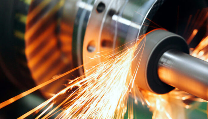
D&X specializes in meticulous wafer precision grinding and thinning services, offering unparalleled customization capabilities. Our partners’ state-of-the-art facilities can adeptly handle wafers of varying thickness, tailoring the process to accommodate specific requirements.
-
Dicing
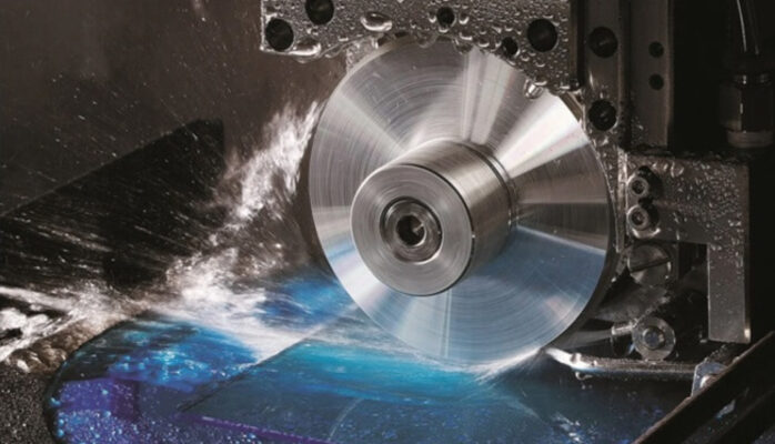
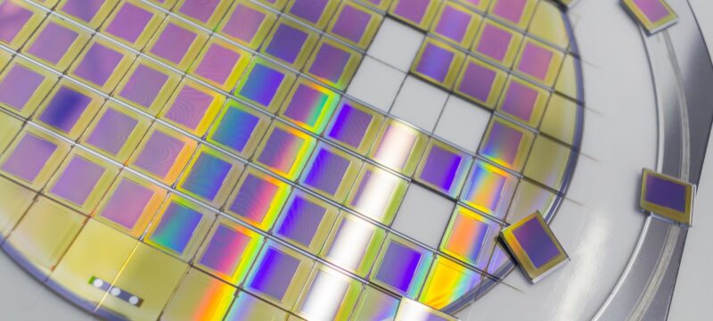
Our advanced wafer dicing service is characterized by precision and flexibility. Our capacity for customized wafer dicing stands as a testament to our commitment to meeting unique client specifications.
-
 Lithography
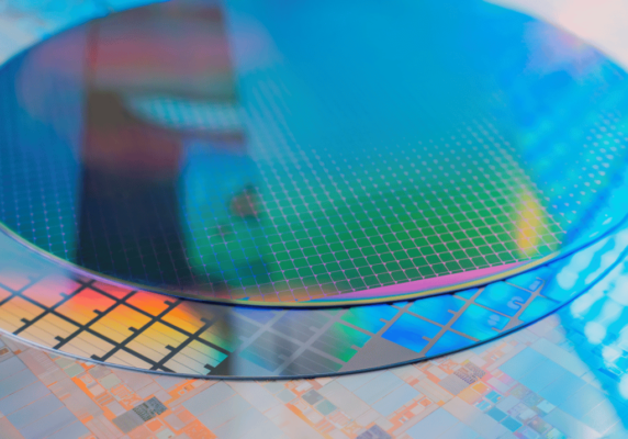
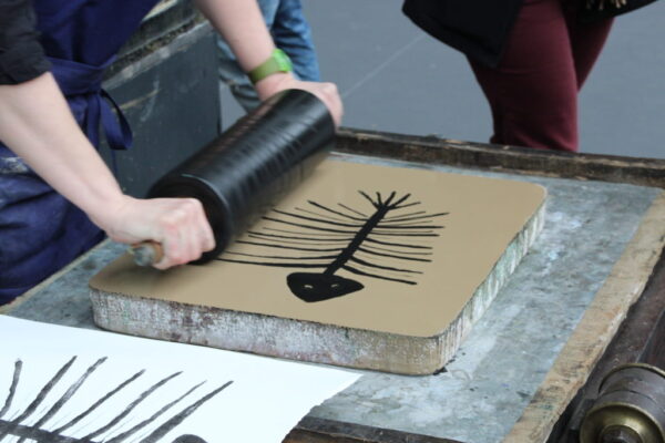
D&X strives to be at the forefront of lithography services, offering a highly customizable solutions that caters to the unique demands of our clients. Wafer lithography is a fundamental process that involves transferring a predefined pattern onto a wafer’s surface.
Lithography
D&X strives to be at the forefront of lithography services, offering a highly customizable solutions that caters to the unique demands of our clients. Wafer lithography is a fundamental process that involves transferring a predefined pattern onto a wafer’s surface.
-
 Bumping
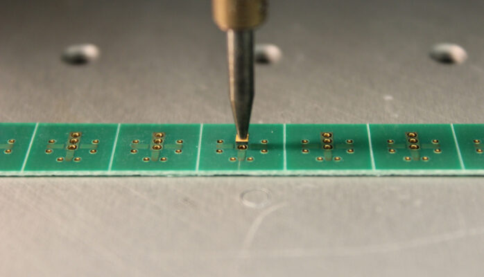
We are also specializing in advanced bumping services, a crucial step in semiconductor manufacturing. This process is also known as flip chip bumping, is a semiconductor packaging process that involves adding metal bumps to the bonding pads on a wafer for subsequent assembly with other semiconductor devices or packaging substrates.
Bumping
We are also specializing in advanced bumping services, a crucial step in semiconductor manufacturing. This process is also known as flip chip bumping, is a semiconductor packaging process that involves adding metal bumps to the bonding pads on a wafer for subsequent assembly with other semiconductor devices or packaging substrates.
-
Bonding
D&X specialized in wafer bonding, a sophisticated semiconductor manufacturing process critical for device integration. This process involves joining two wafers or materials to create a single integrated structure.
-
- Silicon wafer
- Stocklist
- News
- Recruitment
- Contact us
 EN
EN
-
- 0






 ZH
ZH JA
JA
Latest information and special offers
Sign up to receive the latest information from us.